Fabrication of novel light sources on a nanoscale
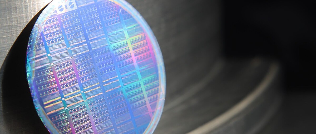
A notable achievement is the development of Structured Micro Illumination Light Engine (SMILE) based on gallium nitride (GaN) technology, using InGaN/GaN microLEDs to emit partially coherent light, essential for chip-based microscopes in life sciences metrology [3, 4]. The scalability of these technologies was demonstrated by a unique microLED array operating at 100 kHz. For blue/UV photonic integrated circuits, aluminum nitride (AlN) is ideal due to its large electro-optical coefficient. QuantumFrontiers has contributed significantly to high-quality AlN fabrication through sputtering/high-temperature annealing [5], understanding defects [6], and addressing parasitic oxide layers during processing [7].


Foundations for the development of ion trap quantum computers
On the crucial topic of integrating quantum systems, QuantumFrontiers has established the inter-institutional initiative “TrapFab” which brings together Leibniz Universität, TU Braunschweig, national metrology center PTB and Laserzentrum LZH. TrapFab has demonstrated a scalable multilayer ion-trap chip technology for quantum processors [8, 9], is developing UV/blue optical waveguide technology for trapped-ion quantum computing and optical frequency metrology and advanced atom chips for metrology and sensing. These activities have triggered important collaborative projects with industrial partners like Infineon, ams OSRAM or Qudora Technologies, to push aspects of the technology towards applications.
This article is part of a series on QuantumFrontiers success stories
Publications
-
Bibliography
[1] A. Tuniz, O. Bickerton, et int, C. M. de Sterke. Modular Nonlinear Hybrid Plasmonic Circuit.
Nature Communications 11, 2413. doi:10.1038/s41467-020-16190-z (2020).[2] A. A. Peshkov, E. Jordan, et int, A. Surzhykov. Excitation of Forbidden Electronic Transitions in Atoms by Hermite–Gaussian Modes.
Annalen der Physik 535. doi:10.1002/andp.202300204 (2023).[3] H. S. Wasisto, J. D. Prades, J. Gülink, A. Waag. Beyond solid-state lighting: Miniaturization, hybrid integration, and applications of GaN nano- and micro-LEDs.
Applied Physics Reviews 6. doi:10.1063/1.5096322 (2019).[4] D. D. Bezshlyakh, H. Spende, et int, A. Waag. Directly addressable GaN-based nano-LED arrays: fabrication and electro-optical characterization.
Microsyst Nanoeng 6. doi:10.1038/s41378-020-00198-y (2020).[5] L. Peters, D. Sergeev, et int, A. Waag. Sublimation behavior of AlN in nitrogen and argon at conditions used for high-temperature annealing.
Journal of Applied Physics 133. doi:10.1063/5.0152054 (2023).[6] L. Peters, C. Margenfeld, et int, A. Waag. A Combination of Ion Implantation and High-Temperature Annealing: The Origin of the 265 nm Absorption in AlN.
physica status solidi (a) 220. doi:10.1002/pssa.202200485 (2022).[7] L. Peters, T. Meyer, et int, A. Waag. Parasitic AlxOyNz surface defects on high-temperature annealed AlN and their role in hillock formation.
Applied Physics Letters 123. doi:10.1063/5.0170006 (2023).[8] A. Bautista-Salvador, G. Zarantonello, et int, C. Ospelkaus. Multilayer ion trap technology for scalable quantum computing and quantum simulation.
New J. Phys. 21, 043011. doi:10.1088/1367-2630/ab0e46 (2019).[9] A. Bautista-Salvador, C. Ospelkaus, M. Wahnschaffe, J. Morgner. Method for producing an atom trap, and atom trap
Patent, DE102018111220B3, EP3791408A1, EP3791408B1, US11264220B2, US2021233756A1, WO2019214863A1 (2021).


